Facilities, Services and Trainings
Reference for quantum, micro and nano technologies
- Qualified personnel of INRiM, Politecnico di Torino e Università degli Studi di Torino;
- Design, fabrication, and characterization of quantum metrology devices;
- Growth, characterization, and processing of micro and nanoscale materials for the fabrication of MEMS, microsensors, and Lab-On-Chip.
Services
- Infrastructure access and training;
- Support to the development of new micro and nanostructured materials;
- Support to the measurement and characterization of devices for on-demand applications;
- Support for the design and development of functional devices and components.
Access mode
- Services provided by internal staff;
- Autonomous or assisted use.
Clean room access trainings
To access the PiQuET facility is mandatory to attend the access training.
INRiM, PoliTo, and UniTo personnel have to fill out the form to the right to pre-book their participation. Two weeks before the training date, the possibility of booking will be disabled. The PiQuET Staff will ask for your confirmation of participation before the training.
People who do not belong to INRiM, PoliTo, and UniTo, please send an e-mail to info@piquetlab.it.
Download the Access fees to services for the External users 2026
Clean room capabilities


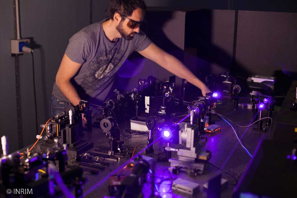
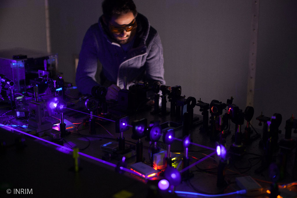


1. Characterization of Quantum Devices
The functionality or principle of operation of Quantum Devices depends on quantum mechanical effects, which are physical phenomena occurring at atomic and subatomic scales. Among quantum technologies, we deal with:
1. Quantum Clocks, which are extremely accurate and precise instruments that measure quantum fluctuations of atoms;
2. Atomic Sensors, that provide RF-fields, temperature, length, gravity, space and geodetic reference;
3. Quantum Electronics, which deals with quantum electrical standards (based and the quantum Hall, the Josephson, and the single-electron-transport effects), quantum-enhanced sensors (e.g. nano-SQUIDS), and RF-based measurement methods and systems for future quantum computers;
4. Quantum Photonics, which investigates optical quantum phenomena at the single-/few-photon level, such as coherence, entanglement and squeezing.
For these technologies, Quantum Metrology can provide (i) general traceability of quantum sensors, and (ii) development of new physical and documentary standards by considering needs from stakeholders in science and technology, industry, economy, and society.
1.1 Optical Cryostats (Cryostation s100 Montana and ATTOCUBE AttoDry800)
1.2 Optical Tables
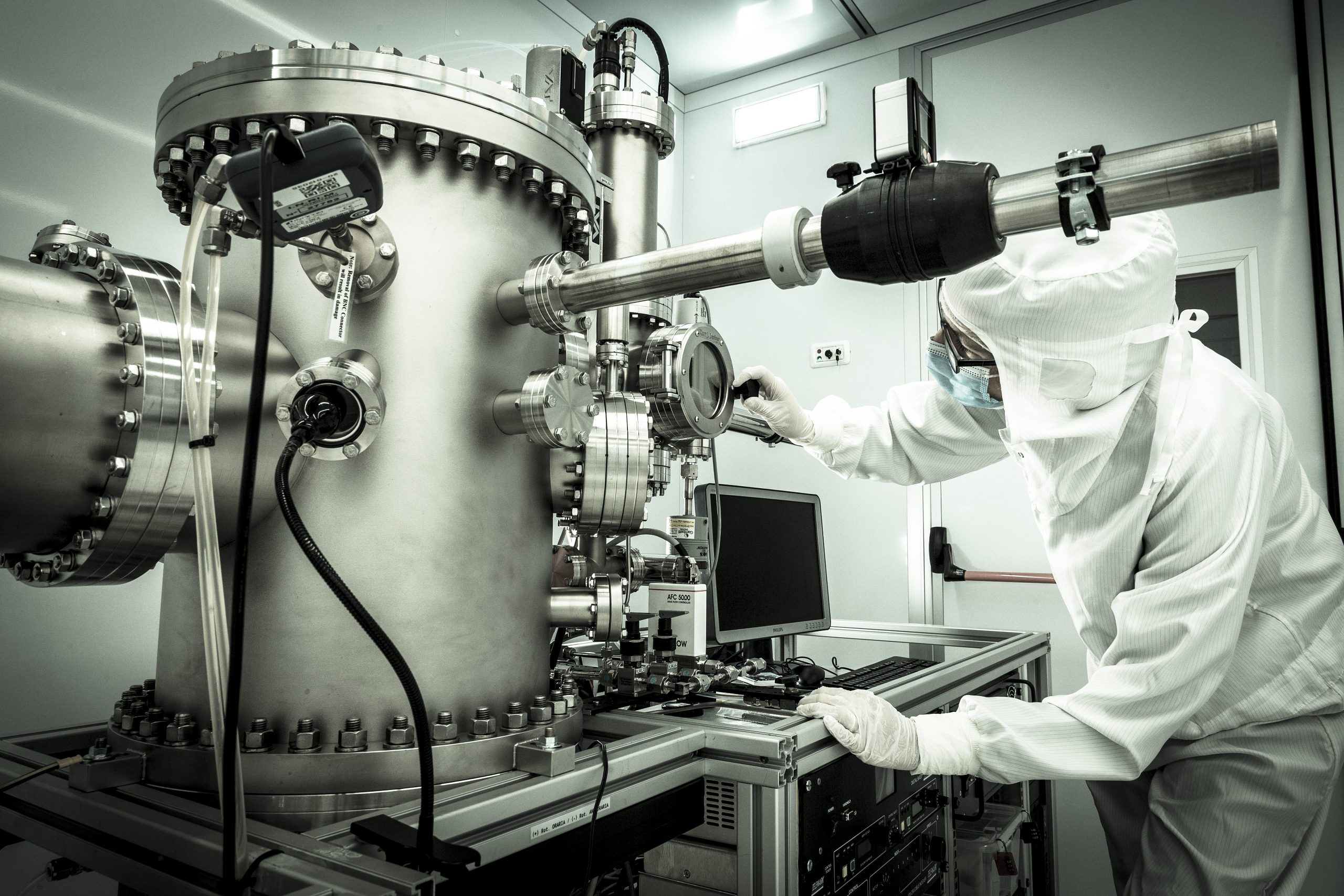
2. Deposition, Growth & Thermal Treatment
We are able to offer several deposition techniques, spanning from evaporation/sputtering of metals and dielectrics to growth of materials, such as oxides, nitrides and polymeric insulators (parylene). A dedicated nano-CVD reactor is also present for the growth of graphene.
The type of deposition depends on the desired material, the film characteristics (thickness, density, grain size, mechanical and/or optical properties), the substrate temperature, and the physical properties (amorphous, polycrystalline, or crystalline).
After deposition, the materials can undergo a thermal treatment, that permits – for instance – to dope or oxide the film or the substrate, or change their chemophysical properties by annealing.
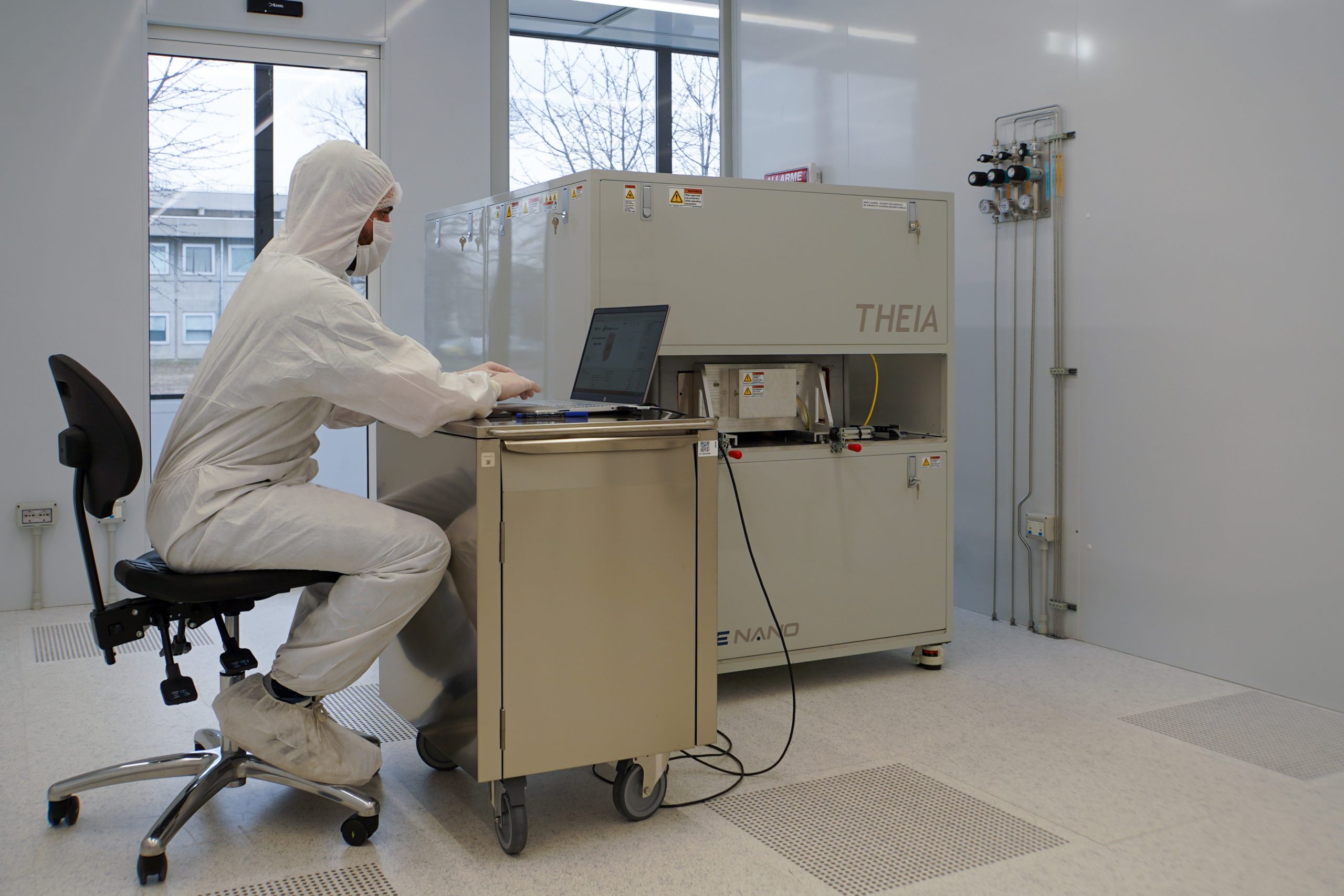
2.1 ALD – Atomic Layer Deposition (Theia and BeneQ)
2.2 Low-Pressure Chemical Vapour Deposition (LPCVD)
2.3 Inductively Coupled Plasma – Chemical Vapour Deposition (ICP-CVD)
2.4 Sputtering Kenosistec
2.5 Hot embossing
2.6 Rapid Thermal Processing
2.7 Parylene coater
2.8 Graphene Chemical Vapour Deposition
2.9 E-gun Evaporator
2.10 E-Beam Telemark


3. Lithography
Lithography is a family of techniques used to transfer two-dimensional (or more seldomly 3D) patterns onto a wafer substrate, by exploiting the change in the chemical properties of a resist polymer (by means of light or focused electron beams) spincoated on the target substrate (e.g. a silicon wafer).
The patterning is achieved through one of two base methods:
- direct writing of the pattern (laser writer, EBL or 2PP)
- transferring the pattern through an optical mask (optical lithography) or stamp (micromolding).
The litography-defined pattern is often the first of a series of steps that lead to the final device, which usually comprises several other subsequent micromachining processes (material deposition, etching, or serial combinations of these).
3.1 Laser Writer (Microtech and Heidelberg)
3.2 UV LED exposure system
3.3 Double side Mask aligner
3.4 Nano Rapid Prototyping System (2PP)
3.5 Electron-Beam lithography (EBL)


4. Etching
Etching techniques include a wide and heterogeneous number of methods used to remove material from previously deposited layers, or from bulk substrates. Among these, we include:
- dry etching methods, which employ chemically active gas plasmas (e.g. for the isotropic etching of bulk silicon wafers, or previously deposited oxides and nitrides) and inert heavy-ion gas plasmas (argon ion beam etching);
- wet etching methods, which employ acid- and alkaline-based solutions for isotropic etching of materials (e.g. etching of thin metal films, thin dielectrics, bulk silicon, etc). These latter are presented in section “5 – Chemical processing”, and are carried out under chemical hoods to guarantee a safe work environment for all users.
5. Chemical processing
Chemical processing involves all wet-chemistry techniques, such as:
- cleaning procedures (e.g. by means of solvents, acid and base solutions)
- processing of materials (by means of wet-etching, e.g. removal of thin layers of metals, dielectrics and semiconductors)
- development and stripping of litographic resists
- electroless deposition and electroplating of thick layers of metals
5.1 Chemical Mechanical Polishing (CMP)
5.2 Chemical hoods (General, Full lithographic benches)
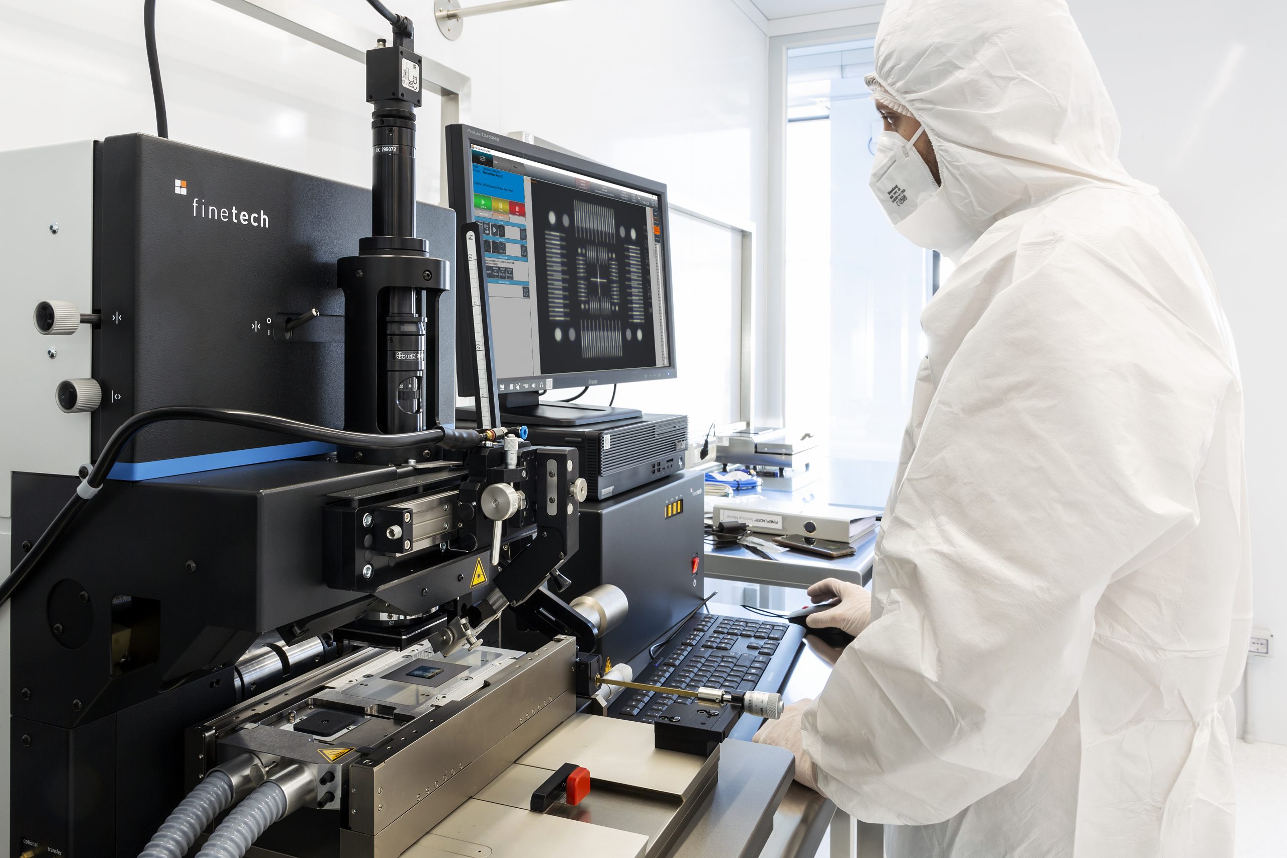
6. Packaging
Packaging techniques involve several different technologies used to separate and isolate the devices from the original micromachined wafer (e.g. dicing), make electrical connections to the external control units (e.g. wire bonding), bond surface-to-surface entire wafers (e.g. wafer bonding) and encapsulate the finished device (e.g. flip chip bonding).
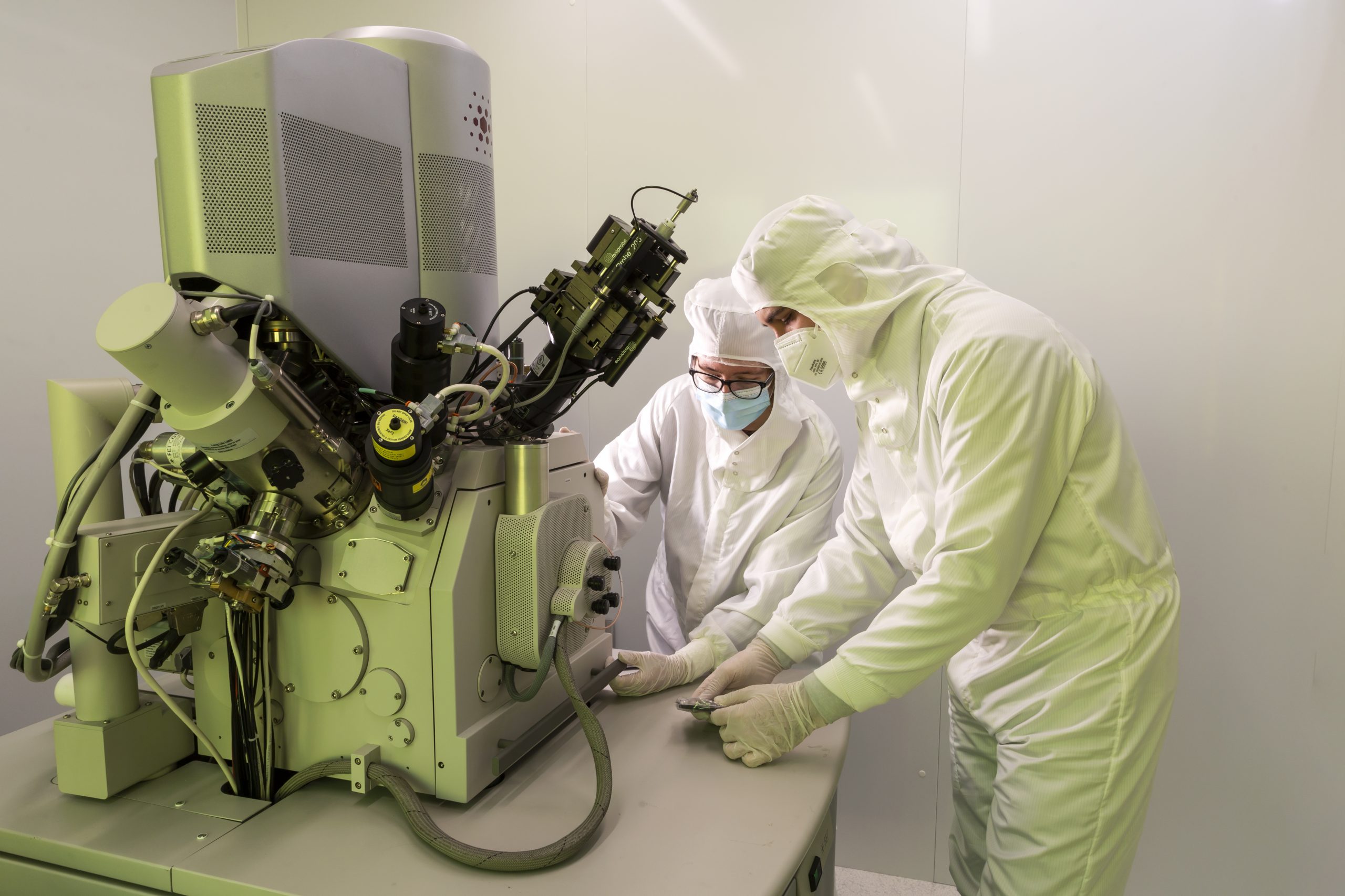
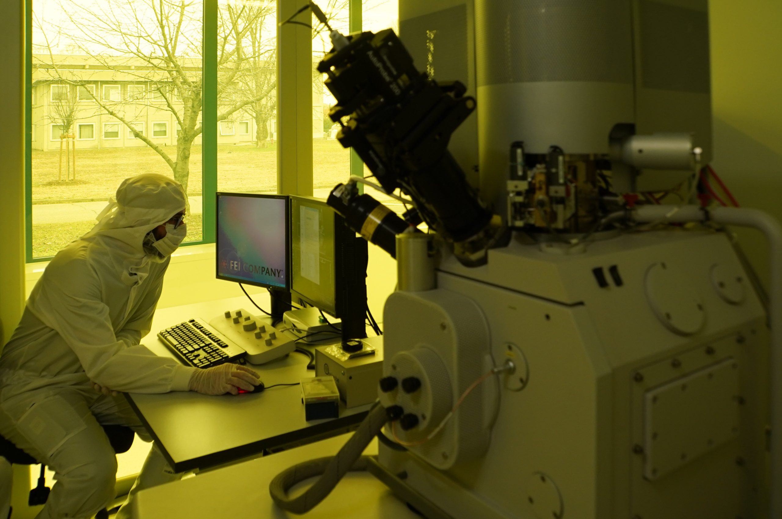

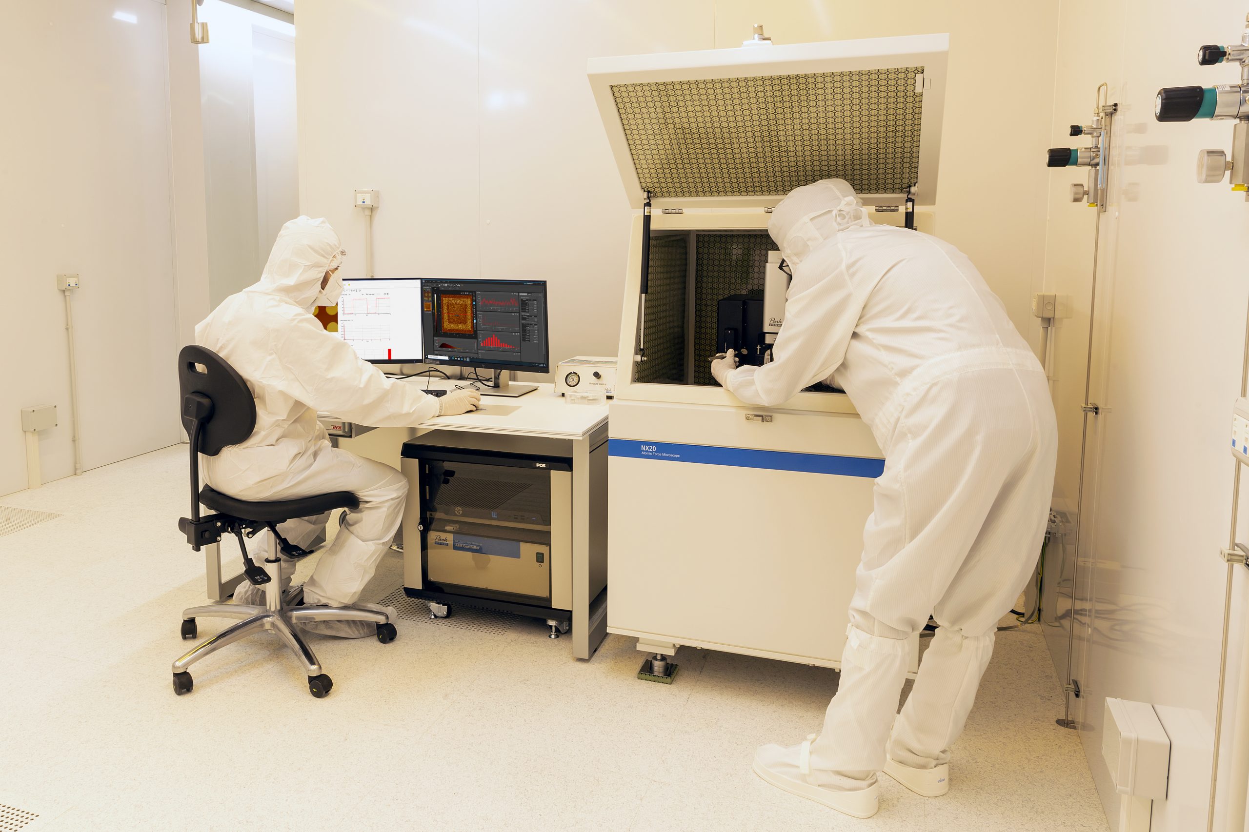

7. Characterisation
Characterisation techniques comprehend all instruments that allow to study the fabricated device, in
particular:
- Surface Topography (roughness, texture) and Physical Dimensions (height, width, pitch, etc.);
- Material Composition (elemental composition);
- Material Physical Properties (e.g. optical, electrical, piezoelectric, magnetic properties).
7.1 Electron Microscopes (Tabletop SEM; Scanning Electron Microscope/Focused Ion Beam (SEM/FIB); Transmission Electron Microscopy (TEM))
7.2 Probe station
7.3 Atomic Force Microscope (AFM)
7.4 Digital microscope
7.5 Ellipsometer
7.6 Stylus profilometer
Additive Manufacturing Laboratory